 |
Now this page is about an work in progress.
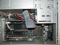
It all started (in 2015 I guess) when I've found an (non-turbo) XT motherboard with an 8088 that was in good condition and and has all ICs in sockets, most big ICs were made by UMC in 1986.
There was no memory in the lower right corner, the BIOS ROM was a rather lackluster one branded MEGA-BIOS from "Display Telecommunications Corporation" dated 1983 which I replaced with an compatible AMIBIOS.
A dump of the old BIOS can be downloaded here.
Ruud's diagnostics ROM revealed that channel 0 of the PIT was defective, which I replaced with an Intel part.
And later I found a 8087 in a gold ceramic package that works (according to the diagnostic ROM).
I've soldered an 14.318MHz oscillator into the clock circuits as I've later bought an discrete full-length CGA clone card which didn't produced the right colorburst frequency due the crystal being way off and I've tried 5 different ones and attempted to add extra caps to get it right without success.
The following is present:
What's missing:
 |
 |
Adrian Black showed one of these CGA6845 cards in this *video* and was rather shocked that this card performed exactly like an original IBM CGA card (with infamous "snow") but that was something I really wanted for my build.
All PCBs of the IBM CGA cards (including the remakes) have that annoying layout where the bottom edge goes down after the ISA connector that prevents the card from being inserted into a 16-bit slot or an motherboard that with socketed ICs like the one I have.
After some research and I found out that the company behind this card has a *website* with *schematics*.
And those showed the exact same color multiplexer used in real card for NTSC chroma modulation, sadly the unused pin for this signal does nothing.
That's why it was necessary to recreate these circuits with extra logic. I used an 74HC4051 instead of 74151 as I didn't had this rare part handy. The colorburst gate is generated via the dual counter 74*393 and diode logic and has the wrong output polarity (compared to IBM schematics) which is compensated by swapping the lines going in to the 4051 multiplexer.
This means that the 80-column color text bug is effectively fixed as my burstgate is derived from the final HSync output and not the HSync from the 6845. Also the phase of the color burst is fixed to the sync signals in the same manner as original, this makes these "NTSC artifact color" tricks used by many games work properly every time while most clone cards (may) get the phase wrong.
Lastly I've added an fuse for 5V to the unused pin on the DE-9 to prevent damage to the 5V traces in case that pin gets shorted to ground, I'll intend to use that for my RGB-SCART adapter.
Here's the schematic for my mod as a monochrome GIF.
And a guide on which pins to connect: 1400x930 - 61,2KB, 700x465 - 18,3KB.
I took some screenshots with my good old STK1160 grabber (uses Chinese clone of Philips SAA7113).
Last minute change: all PNGs were over 3MB in size, that's why I omitted these for now.
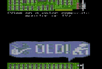
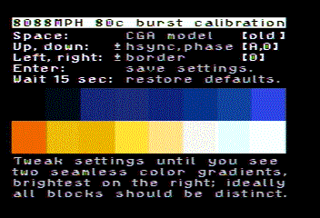
The CGA Compatibility Tester looked pretty good and that with the default hue setting.
I don't know why my grabber loses sync on the CGA determination screen, that's why the screenshot looks so jacked up. My TV has no trouble displaying that. The setup of 8088MPH looks okay.
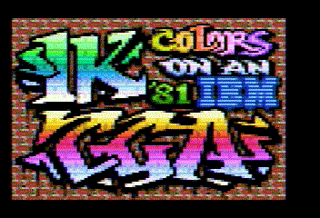
The graphics look amazing and spot on. Telling these apart from the original IBM card is quite though.
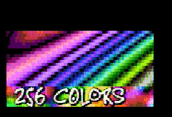
So far, everything looks fine. The sprite demo is very impressive considering what CGA is designed for.
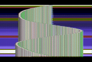
The "flower girl" image looks a bit too yellow to me but the copperbar effect is 100% working on this card.
Something I couldn't say for the other CGA clone card that has shorter waitstates thus that effect is broken on that card (and any other system for that matter that runs a tad faster than a stock IBM 5150)
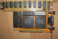
This is the current state.
I'll still need to create the schematics for this one.
These four oddball chips are 4x128KByte SRAM with an address decoder hidden in the inside, these neat packages are pin compatible to 512KByte SRAMs.
There will be empty space near the connector if I want to add FIFO UART and Bi-directional LPT ports.
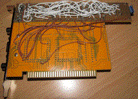
The old junk cards where I cut the ISA connector from where already very broken.
(one was a crappy modem with cracked PLCC ASICs and the other some sort of 80186 SBC snapped in half)